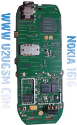
Nokia 1616 Full PCB Diagram Mother Board Layout.
Here is the diagram of Nokia 1616 PCB.so i will add some more diagram in high resolution so that you can add some more repairing trick for

Thanks
Disclaimer.these images are uploaded by website visitors.and for teaching and study purpose so we will not be responsible for any damage in your mobile it is your responsibility to use the method as mentioned in the posts.and if any diagrams is your own and you do not want to be on this site please contact us at Contact Us and the diagram will be removed from site as soon as possible.
Here is the diagram of Nokia 1616 PCB.so i will add some more diagram in high resolution so that you can add some more repairing trick for

High Resolution
Download High Resolution Diagram of Nokia 1616
Nokia 1616 if you find some new repairing techniques please must email me and i will post that diagram with your reference in this way we all make it possible “REPAIRING MADE EASY” the basic point of www.u2ugsm.comThanks
Disclaimer.these images are uploaded by website visitors.and for teaching and study purpose so we will not be responsible for any damage in your mobile it is your responsibility to use the method as mentioned in the posts.and if any diagrams is your own and you do not want to be on this site please contact us at Contact Us and the diagram will be removed from site as soon as possible.


 12:47 AM
 ramesh ahir

0 ટિપ્પણી(ઓ):
ટિપ્પણી પોસ્ટ કરો